Description
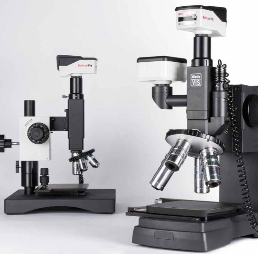
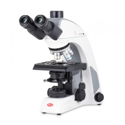
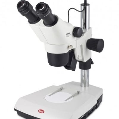
Motic Microscopes VIS100-E & VIS 200 Digital Inspection Semiconductor Microscope
Monocular digital camera compound microscope with Long Working Distance (LWD) Objectives. High magnification digital microscope for microelectronics wafer inspection. Long working distance objectives. Avoid inspection damage to silicon wafer / chip surface / wire bonding.
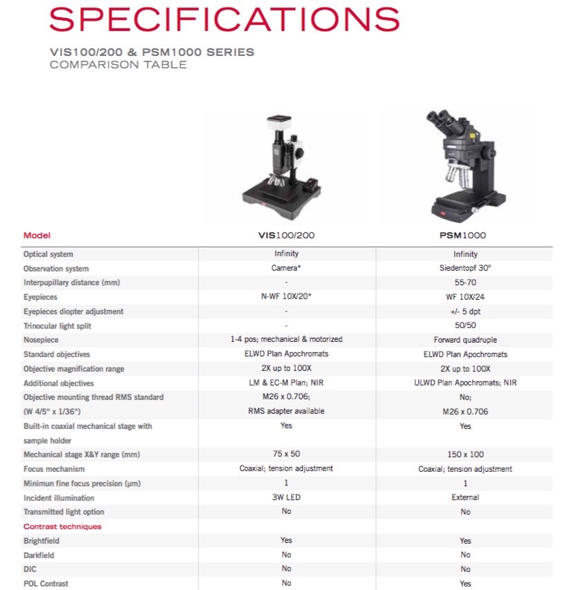
MOTIC MICROSCOPES VIS-100-E
- Video Inspection system with uniaxial optical design
- 5 position nosepiece for LM Plan Objectives
- 3W LED fiber-optic coaxial illumination (6000K~7000K color temperature) with aperture diaphragm
- 1.0X C-mount camera adapter (no-lens, un-focusable) 38mm mount compact control box with intensity adjustable
MOTIC MICROSCOPES VIS200-A
- Video Inspection system with uniaxial optical design
- Vertical upright image port for strong power laser (1064, 532, 355nm)
- Or additional camera and side port with 1.0x C Mount camera adapter
- 3W LED fiber-optic coaxial illumination with aperture diaphragm
- 1.0X C-mount camera adapter (no-lens, focusable) 38mm mount compact control box with intensity adjustable
- 4 position revolving nosepiece
- Note :-
- No objectives, no eyepieces & stand are included in above basic package.
- Motic PSM 1000 / VIS Series LWD Objectives Here
- Contact MMS Microscopes or Request a Quotation Here
